image image image image image

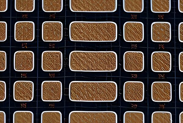
Patterned Deposition

Szimpla offers single-step patterned deposition equipment for the semiconductor industry. Instead of traditional lithography followed by deposition, our patent pending system allows for material to be deposited directly in the desired pattern, streamlining the process into one step.

image image image

Discover Key Applications

image1

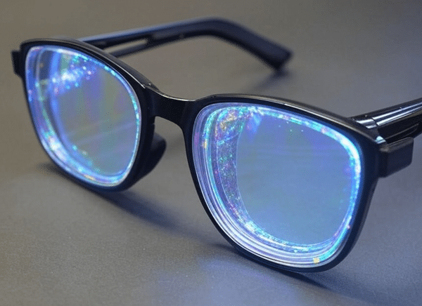
Waveguides and Optical Filters 

Szimpla's 3D patterning capabilities are especially suited for developing complex photonic structures like waveguides, optical filters and sensors.
image2
Communications and Mixed Signal SoC Drastically reduced design cycles and elimination of NRE costs, enables rapid prototyping of complex SoCs, accelerating time-to-market with lower costs.
PlaceholderImage1314
Advanced Sensors and Devices Our low-cost fabrication and rapid prototyping, allows for new sensor designs, with improved performance metrics and reduce development timelines.